
P25Q10L
The P25Q10L is an Ultra Low Power,1M-bit Serial Multi I/O Flash Memory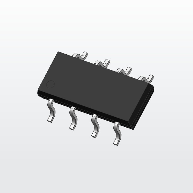
 P25Q10L.PDF
 …ΧΤΖ–≈œΔ
The P25Q10L is a serial interface Flash memory device designed for use in a wide variety of high-volume consumer based applications in which program code is shadowed from Flash memory into embedded or external RAM for execution
P25Q10L’s Features
1. Single 1.65V to 2.0V supply
2. Industrial Temperature Range -40C to 85C
3. Serial Peripheral Interface (SPI) Compatible: Mode 0 and Mode 3
4. Single, Dual and Quad IO mode
- 4M/2M/1M/512K x 1 bit
- 2M/1M/512K/256K x 2 bits
- 1M/512K/256K/128K x 4 bits
5. Flexible Architecture for Code and Data Storage
- Uniform 256-byte Page Program
- Uniform 256-byte Page Erase
- Uniform 4K-byte Sector Erase
- Uniform 32K/64K-byte Block Erase
- Full Chip Erase
6. Hardware Controlled Locking of Protected Sectors by WP Pin
7. One Time Programmable (OTP) Security Register
- 3*512-Byte Security Registers With OTP Lock
8. 128 bit unique ID for each device
9. Fast Program and Erase Speed
- 2ms Page program time
- 8ms Page erase time
- 8ms 4K-byte sector erase time
- 8ms 32K-byte block erase time
- 8ms 64K-byte block erase time
10. JEDEC Standard Manufacturer and Device ID Read Methodology
11. Ultra Low Power Consumption
- 0.1uA Deep Power Down current
- 9uA Standby current
- 2.5mA Active Read current at 33MHz
- 3.0mA Active Program or Erase current
12. High Reliability
- 100,000 Program / Erase Cycles
- 20-year Data Retention
13. Industry Standard Green Package Options
- 8-pin SOP (150mil/200mil)
- 8-land USON (2x3mm)
- 8-land WSON (6x5mm)
- 8-pin TSSOP
- WLCSP
- KGD for SiP
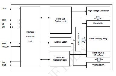
P25Q10L’s Block Diagram
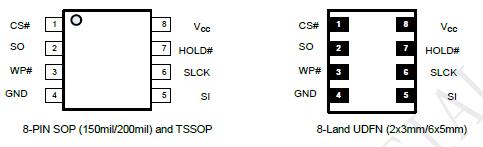
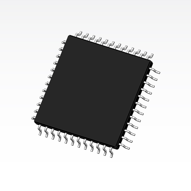
P25Q10L’s Package
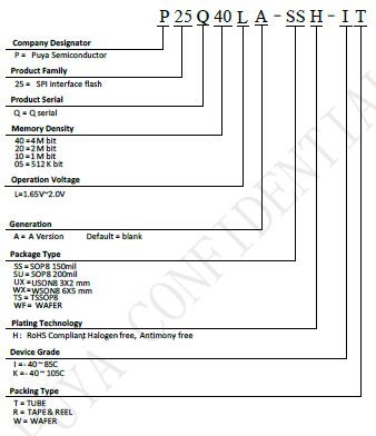
P25Q10L’s Ordering Information
»γΚΈΙΚ¬ρ
‘ΎœΏΉ…―·
Ϋ®“ιΝψ έΦέΗώΫω”Ο”Ύ‘ΛΥψΘ§“‘‘ΣΈΣΒΞΈΜΘ§≤Δ«“ΦέΗώ «ΗΓΕ·ΒΡΓΘ »τ“Σ≤ι―·”–ΙΊ≈ζΝΩΦέΗώΓΔ±ΨΒΊΜ豓ΦέΗώΜρΫΜΗΕ±®ΦέΒΡ–≈œΔΘ§«κ”κΙΪΥΨΝΣœΒΓΘΘ®ΒψΜςΉ…―·Θ©
ΒψΜς’βάοΗχΈ“ΖΔœϊœΔΝΣœΒΖΫ Ϋ
“ΒΈώΒγΜΑΘΚ0755/23141725 18576699326
“ΒΈώQQΘΚ2335804557¥Ϊ’φΘΚ0755/23141201
QQΘΚ2286874832Θ®ΖΫΑΗΘ© 1762516767Θ®ICΘ©
” œδΘΚsunnyqi001@126.com
ΒΊ÷ΖΘΚ…νέΎ –±ΠΑ≤«χΈςœγ–¬Κΰ¬Ζ”κάΆΕ·¬ΖΫΜ≤φΩΎ±ΠΫίΑ≤Ψ≠Ο≥÷––Ρ503Θ®¬ό±ΠœΏΤΚ÷όΒΊΧζ’ΨB≥ωΩΎΘ©
ΙΪΥΨΙΌΆχΘΚhttp://www.sunnyqi.com/
―υΤΖΦΑ―·Φέ
Ϋ®“ιΝψ έΦέΗώΫω”Ο”Ύ‘ΛΥψΘ§“‘‘ΣΈΣΒΞΈΜΘ§≤Δ«“ΦέΗώ «ΗΓΕ·ΒΡΓΘ »τ“Σ≤ι―·”–ΙΊ≈ζΝΩΦέΗώΓΔ±ΨΒΊΜ豓ΦέΗώΜρΫΜΗΕ±®ΦέΒΡ–≈œΔΘ§«κ”κΙΪΥΨΝΣœΒΓΘΘ®ΒψΜςΉ…―·Θ©
έΚσΖΰΈώ
…ΘΡαΤφΩΤΦΦ «…νέΎ –÷ΣΟϊΒΡIC¥ζάμ…ΧΘ§ΡήΈΣΙψ¥σΙΛ≥Χ Π”κ≤…ΙΚ≈σ”―ΧαΙ©÷ΎΕύάύ–Ά≤ζΤΖΘ§–Γ≈ζΝΩΒ±ΧλΫΜΜθΘ§10K“‘…œ5-10ΧλΫΜΜθΓΘ
œύΙΊ≤ζΤΖ


- ΩΆΖΰ»»œΏΘΚ
0755-23141725 -
IC≤ζΤΖΉ…―·
-
ΖΫΑΗΉ…―·
- …νέΎ –…ΘΡαΤφΩΤΦΦ”–œόΙΪΥΨ
- “ΒΈώ»»œΏ: Υοœ»…ζΘΚ18576699326/ QQ:2335804557 ¥Ϊ’φΘΚ86-0755-23141201 ” œδΘΚsunnyqi006@126.com
-
’Ϋ¬‘ΚœΉςΦΑ≤…ΙΚ»»œΏ:
Υοœ»…ζΘΚ13510901648/ QQ:2361879025
 “ΒΈώΈΔ–≈
 ’Ϋ¬‘ΚœΉςΈΔ–≈